Research
Laser cleaning and surface modification
Laser cleaning technology to remove particles from surfaces has long been an issue of practical and scientific importance due to its potential to removal sub-micrometer-scale contaminant particles. Various laser cleaning processes based on different physical mechanisms have been proposed depending on industry needs, e.g., dry laser cleaning (DLC), steam laser cleaning (SLC), laser shock cleaning (LSC), and laser-induced spray jet cleaning (LSJC).
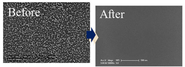
SEM images of silicon wafer contaminated with 300 nm sized PSL particles
Laser micromachining
Laser is good tool for micromachining because of its characteristics of noncontact, and precise machinability. Many laser processing such as cutting, drilling, annealing and surface modification were widely used for metal, ceramics and other materials. Especially, ultrafast laser, which have pulse length lees than hundreds of picosecond, have fine processing size and minimal heat affected zone, using nonlinear behavior generated by short pulse length and high peak power of ultrafast laser. Finding correlation between process parameters and machining, and optimization of process for fabricating high precision micro-sized structures without defects in case of using various lasers and materials has been studied for various applications and industry fields such as MEMS, micro fluidics, semiconductor, display, and etc. UV laser polymer projection machining was using photochemical effects to remove the polymer with certain shape. Selective removal of polymer, machining complex shape, and micro pillars were studied. Ultrafast laser was used to fabricate the hard-to-fabricate materials, serveral micron sized structures, or to machine the materials with minimal thermal effects. Selective machining of multi-thin-layers, whose thickness of each layer less than 1 μm, using femtosecond laser was conducted.
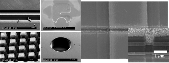
Polymer projection machining (left) and selective machining of multi-thin-layer (right)
Laser sintering
Transparent conductive oxide (TCO) has high transmittance and conductivity which can be applied in many practical devices. Current fabrication method for this material, represented by sputtering has some problems of material waste and complex set-up. In this study, we developed a new method using indium tin oxide nano-particle coating method and pulsed laser sintering for fabricating thin transparent conductive film.
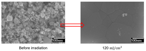
SEM images of ITO film before and after laser sintering
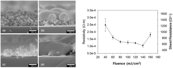
Cross sectional view of the ITO thin film after laser sintering (left) and variation of electrical resistivity of the film with laser fluence (right)
Metal 3D printing
Powder bed fusion (PBF) has attracted significant attention across various fields as a manufacturing technique for producing three-dimensional (3D) metallic structurese. The AM method can produce complex, high-resolution structures, including parts with lattice or porous structures, biocompatible implants, and thin-walled components.
.png)
3D printing systems
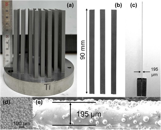
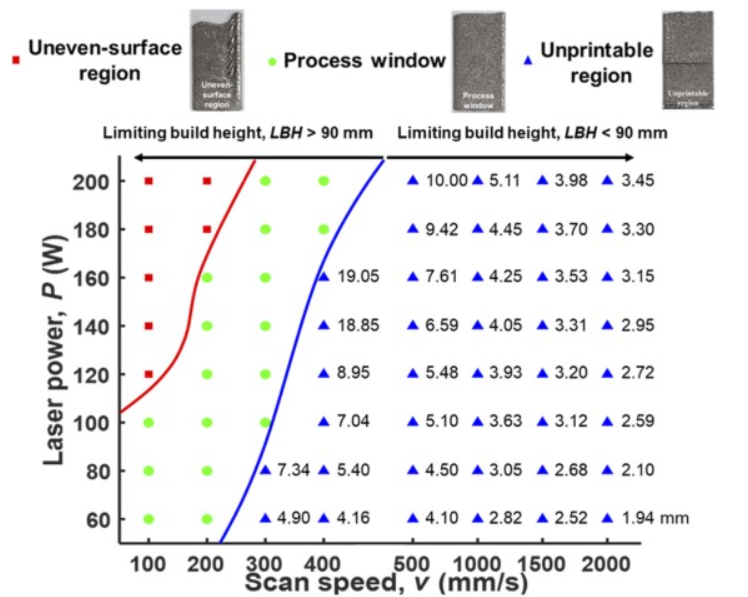
Thin walls fabricated PBF (left) and process window of thin-wall fabrication of laser power and scan speed (right)
Modeling and simulation of 3D printing process
Residual stresses generated during PBF process mainly arise from the thermal gradients and cooling rates. Laser parameters such as power and scanning speed determine the size and temperature of the melt pool, subsequently affecting the thermal gradient and cooling rates. Optimizing laser process parameters, such as hatch spacing, build orientation, and layer thickness, as well as incorporating support structures, can provide control over thermal gradients and cooling rates, thereby influencing residual stress formation. Therefore, the melt pool characteristics and residual stress distribution were investigated through simulation of the 3D printing process.
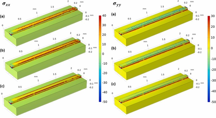
Comparison of sigma xx and sigma yy residual stresses for (a) No IR, (b) IR at 100 ºC, and (c) IR at 300 ºC after the parts were cooled to room temperature.